A few years ago, in the middle of a fairly severe burnout, I tried to motivate myself the way a sensible adult would: by living on YouTube. I had caught the BenEater bug and decided that what I really needed in my life was a breadboard Z80 computer.
It worked. Mostly. My DIY projects are characteristically held together by the surface tension of a spilled can of Monster.
I called this contraption Ataru. It booted. It ran code. It blinked LEDs. I had grand plans: serial comms, graphics, sound, maybe even games. Because at the end of every engineering rainbow, there’s a stash of video games, and that’s the real objective.
Unfortunately, though I live for video games, I do not live alone. My desk has the spatial density of a zip file that refuses to decompress. There is no room for a permanent silicon battlefield of jumper wires and electronic components. At one point, I was gently informed that the breadboard Waterloo needed to be evacuated. This was not a war I could win.
So Ataru went into a box.
Fast forwards a few months ago. I decided it was time for a resurrection. I opened the box, stared at the nest of wires, and briefly considered that one resurrection in human history was probably sufficient. This was Ataru, not Lazarus, after all.
I mean, I tried to revive it; breadboard wire slid under my fingernail and delivered immediate divine feedback. I decomposed the computer instead.
I went to sleep.
At some ungodly hour of the night, I woke up to music playing in my office (where Waterloo happened). Forty years in, and Microsoft still hasn’t figured out how to make a computer sleep properly. My retro maker playlist was looping in the dark like a sign from the gods of marginal signal integrity.
Clearly, this was it. Ataru needed a reboot.

Design Principles
Determined to avoid the pitfalls of breadboard computing, I decided to try something radical for once: act like an engineer.
To my engineer friends: as a computer scientist, I apologise in advance if this offends you, or so you’d think I’d say.
I started listing what I actually wanted from this build. Modularity was at the top. I wanted independent modules like clock/reset, CPU, memory, I/O; I wanted to be able to reason about these in isolation – separation of concerns, one might say. I also wanted to minimise trial-and-error chaos. This meant thinking through the design properly on paper, modelling circuits where possible, and not discovering fundamental mistakes through the smell of burned epoxy.
Having absolutely zero soldering finesse, I also wanted to cut back on that. Through-hole components only. No surface-mount malarkey. If a chip didn’t come in DIP, it probably wasn’t invited.
A Modular Approach
I sketched out the basic modules I wanted:
- A clock module with adjustable frequency
- A proper reset circuit that behaves like the Z80 data sheet expects it to
- CPU board with RAM and ROM
- Display module
- Some form of storage or cartridge interface
- And, inevitably, sound, because I am predictable.
The clock/reset board was the first serious piece of work. I modelled parts of it in Falstad. My original ambition included single-stepping support. In a moment of remarkable confidence, I convinced myself that simply slowing the Z80 clock down would effectively give me single-step control. It turns out that’s about as effective as trying to stop time by holding the hands of a grandfather clock.
The Z80 doesn’t politely execute one instruction per visible clock when you slow it down. It still runs continuously. Just more slowly and without proper gating and control logic. “Single stepping” becomes “why isn’t this working?”
So I recalibrated. By which I mean I read more documentation about how the Z80 actually works. After a brief discussion with my inner committee, we agreed that the sensible option was clarity: a clock generator capable of full speed or divided frequencies, paired with a reset circuit that produces a clean, Z80-approved, reset pulse.
If I ever want proper single-step logic, that can be a separate module in the future.
That’s the power of modularity.
And procrastination.
Breadboard Trauma
I built the first iteration of the clock/reset circuit on a breadboard. It was educational, but not in a pleasant way – much like one of my lectures.
Breadboard debugging has a particular flavour: intermittent contacts, marginal pull-ups, and wires that look connected but are spiritually opposed to conduction. At some point I was spending more time reseating and uncrossing jumpers than thinking about design.
That was the turning point.
I decided to learn KiCad properly and design real schematics and PCBs. Not because it was strictly necessary, or because I was suddenly possessed by discipline, but because my wife was threatening to call an exorcist; apparently the sheer vocabulary density of my frustrations was starting to peel paint off the walls.
KiCad seemed like the cheaper option.


The First Module
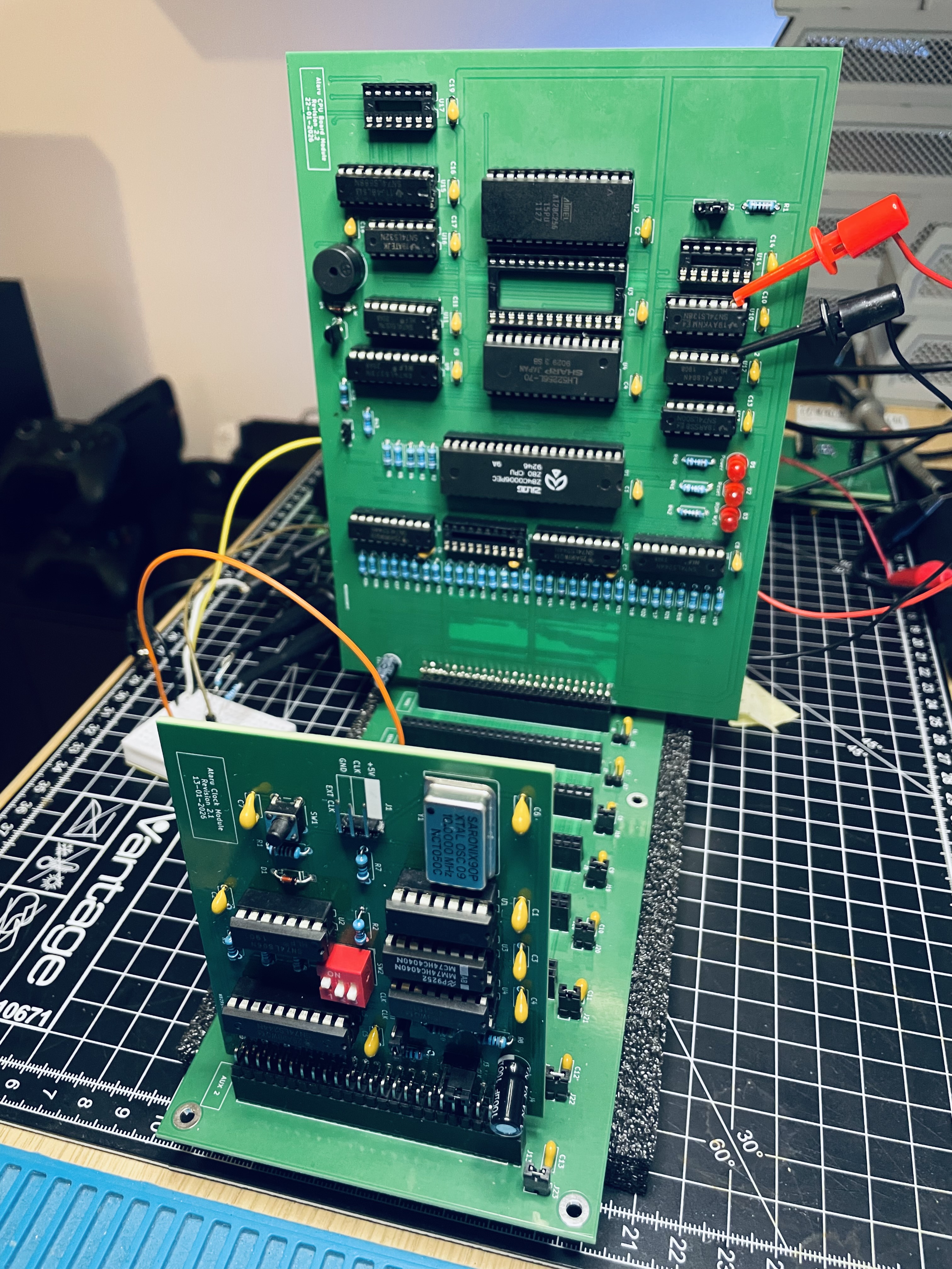
The clock/reset module became the MVP of the project. It was my excuse to learn KiCad (“learn” is doing a lot of heavy lifting here), and design my first proper PCB. I sent the files to PCBWay and experienced the very specific joy of receiving a professionally fabricated board in the mail that contained mistakes I personally designed.
The board exposed five signals: RESET, VCC, GND, CLK and a divided clock selectable via DIP switches.
The divider itself is simple. A binary counter increments at the main clock frequency. Each bit of that counter toggles at half the frequency of the previous one – bit 0 at f/2, bit 1 at f/4, bit 2 at f/8, and so on. A multiplexer selects which counter bit is routed to the output. The DIP switch acts as a three-bit selector.
I soldered the board together “quickly”, meaning within a week and with a growing appreciation for fume extraction. Pro tip: buy an extractor. The noise annoys people, but they won’t stick around to complain.
I connected the board to my oscilloscope and powered it up. The clock signal was… dramatic.
On the oscilloscope, the edges were followed by shadows, not unlike Alucard’s afterimages in Symphony of the Night. Except in this case they were not stylistic. They were ringing. Bad ringing.
After some ritualistic probing, I found the culprit: I had forgotten to route a supply connection from a decoupling capacitor to one of the ICs. The chip wasn’t powered properly. Instead of clean edges, I had created a small RF experiment.
Fixing that trace fixed the waveform. I learned two important lessons: first, DRC is your friend. Second, check your power nets before suspecting cosmic interference.

The Backplane
With a stable clock/reset board, I was ready to design the CPU module: Z80, ROM, RAM and the inevitable jungle of supporting logic and wires. In a moment of either confidence or madness, I skipped the breadboard phase entirely and went straight to KiCad. The decision forced an uncomfortable question: how were these modules going to talk to each other?
The accidental inspiration came from an Arduino GPIO expansion board that I had lying around. It wasn’t elegant but demonstrated the idea of a central board with headers into which other boards could plug. In more respectable terminology, this is called a backplane. Yes, yes, this is the same idea as PCI Express connectors; hindsight is 20/20.
Designing the backplane required actual thinking. A PCB is not something you can “recompile” after routing. I had to decide what signals were global, what belonged to individual modules, and what flexibility was worth preserving. My first instinct was: export everything. If a signal existed, it probably deserved a pin. Bigger felt better.
The CPU board
I settled for a five-slot backplane, with 2×25-pin headers. The next obvious step was design the CPU board and give it a matching connector. In retrospect, I did not lock the CPU board design early. It evolved as it went along, which is euphemism for I kept redesigning it. Eventually, it got tiring, again, euphemistically speaking, so I took a step back and tried to generalise. Notebook out, I listed what I wanted.
At minimum: 32 kB of ROM and 32 kB of RAM. The Z80 has a 64 kB address space, so this split is clean and convenient.
But 32 kB of RAM is modest. As in, game-limiting modest. So I added another 32 kB of RAM that could replace the ROM in the lower half of the address space. That worked, but it raised a practical issue: if the monitor lives in ROM, swapping it out means either copying it to RAM first or constantly flipping between ROM and RAM.
That felt inelegant (read: not complicated enough).
So I refined the idea; instead of treating the lower 32 kB as a single block, I partitioned it into two 16 kB windows. Each window can be independently mapped to ROM, RAM, or something external.
This is where the design became interesting (read: close to complicated enough).
I also wanted the option to boot from external memory, like a cartridge, without copying code into RAM first. Or to memory-map parts of a future display module. So the CPU board needed to support external ROM and RAM, not just its own local versions. To keep the terminology sane:
- A window is one of the 16 kB partitions in the lower 32 kB
- Each window is controlled by 2 bits:
- 0 -> ROM
- 1 -> RAM
- 2 -> External Memory
- 3 -> Reserved
Separately, I defined a bank, also 2 bits wide, allowing selection of one of four banks. This makes it possible for multiple memory mapped devices to coexist on the backplane.
All of this configuration, window selection, bank selection, even the ability to flash ROM, represents CPU state. It must persist independently of memory contents. So I added an 8-bit control register to the CPU board to hold this state. On reset, the system defaults to 32 kB of ROM at $0000 and 32 kB of RAM at $8000.
I also added the ability to flash the onboard ROM. To prevent accidental self-destruction, ROM writes are gated behind a physical jumper. Software alone cannot corrupt the ROM unless I explicitly allow it.
Then came the routing. In Greek, this is known as Nostoi. It’s a fitting term, as it refers to a homecoming journey so fraught with peril, madness, and divine spite that by the time you actually reach your destination, you’re unrecognisable to your family and your dog is the only one who remembers your name.
And I don’t even have a dog.
Nothing could have prepared me for this Odyssey. If you design and route PCBs for a living, I salute you. It took me a week to route what is objectively, a simple two-layer board. I was reminded of Richard Burton’s narration in War of the Worlds:
In the cellar was a tunnel scarcely ten yards long, that had taken him a week to dig…
I suddenly understood the gulf between ambition and competence.
The PCB Trinity
With the newly designed PCBs – the clock/reset board, which now looked less like a banquet table and more like a credit card, the CPU board, which looked suspiciously professional; and the backplane, which looked like a backplane – I was ready to have them fabricated.
This is where I discovered a KiCad plugin that generates production files and pushes them to PCBWay in a single click.
I became a very happy gerbil.
The boards arrived in about a week. I was excited, so I started soldering immediately.
Months later, I still am.
Joking.
Once the clock and backplane were assembled, I ran some basic tests. Everything worked perfectly, giving me a feeling of elation. That’s a dangerous feeling.
I moved on to the CPU board; I soldered everything, powered it up and waited for magic. The only thing that moved was the control register. In my eagerness to devise a clever memory addressing system, I had forgotten to add proper gating logic. The control register was being written far more often than intended. It turns out that “every time the CPU does anything” is not a valid write condition.

This is how I was introduced to bodges.
There is a particular rite of passage in hardware design: soldering wires directly onto a freshly manufactured PCB and fixing them in place with hot glue. In that moment, I felt like a real engineer. There’s nothing like the smell of hot glue in the morning.
This first mistake was corrected with a small mod board. To celebrate the successful patch, and introduce some signs of life, I built a second mod board with a passive buzzer connected to a spare control register bit called AUX_CTL. It buzzed when I wrote to it.
This small indulgence later evolved into a permanent buzzer on the Rev B CPU board.
The second mistake was subtler. I had wired the octal bus transceiver as if data would only ever travel in one direction. That assumption held until I attempted to connect a Z80 CTC in preparation for serial communication.
Eventually, I figured it out. The realisation was not immediate. Language is deceptive that way.
Interrupt controllers, I discovered, are not passive participants; they have opinions about bus ownership. Having been chastened by the Z80 Penates, I decided to treat interrupts with the respect they demand, and implemented hard-wired, daisy-chained priority lines on the backplane. This ensures interrupts are handled by design rather than miracle.
Rev B
It was time to print the boards again.
This revision was sponsored by PCBWay, who generously covered the fabrication and postage costs. Having professionally manufactured boards made the difference between “interesting prototype” and “something I’m not embarrassed to photograph.”

We are now finally in a position to answer the only question that truly matters:
Can this Z80 computer play Doom?
Well, sort of.
There is no graphics engine. No PCM audio. No ray casting.
But there is a passive 5V buzzer.
That will do.
Next
What lies in store for Ataru? I have no idea; I’m a computer scientist, not a fortune teller. What I do see is a backplane with eight empty slots staring back at me. That kind of asymmetry is an affront to my sensibilities.
Playing the Doom E1M1 theme on a buzzer is a victory, but it’s a lonely one. It doesn’t constitute a conversation.
So next comes serial communication. Ataru needs a voice, even if it’s only to complain in a terminal.
Leave a Reply